8255 Programmable Peripheral Interface
Features:
- 3 8-bit IO ports PA, PB, PC
- PA can be set for Modes 0, 1, 2. PB for 0,1 and PC for mode 0 and for BSR. Modes 1 and 2 are interrupt driven.
- PC has 2 4-bit parts: PC upper (PCU) and PC lower (PCL), each can be set independently for I or O. Each PC bit can be set/reset individually in BSR mode.
- PA and PCU are Group A (GA) and PB and PCL are Group B (GB)
- Address/data bus must be externally demux'd.
- TTL compatible.
- Improved dc driving capability
| The 8255A is a programmable peripheral interface (PPI) device designed for use in Intel microcomputer systems. Its function is that of a general purposes I/O component to Interface peripheral equipment to the microcomputer system bush. The functional configuration of the 8255A is programmed by the systems software so that normally no external logic is necessary to interface peripheral devices or structures. |
Data Bus Buffer |
| This 3-stable bi-directional 8-bit buffer is used to interface the 8255A to the systems data bus. Data is transmitted or received by the buffer upon execution of input or output instructions by the CPU. Control words and status information are also transferred through the data bus buffer. |
Read/Write and Control Logic |
| The function of this block is to manage all of the Internal and External transfers of both Data and Control or Status words. It accepts inputs from the CPU Address and Control business and in turn, issues commands to both of the Control Groups. |
|
(CS) Chip Select. A “low’ on this input pin enables the communication between the 8255A, and the CPU. |
|
(RD) Read. A “low” on this Input pin enables the 8255A to send the data or status information to the CPU on the data bus. In essence, it allows the CPU to “read from the 8255A. |
|
(WR) Write. A. “ low” on the input pin enables the CPU to write data or control words into the 8255A. |
| (A0 and A1) |
| Port Select 0 and Port Select 1. The Input signals, in conjunction with the RD and WR Inputs, controls the selection of one of the three ports or the control word registers. They are normally connected to the least significant bits of the address bus (A0 and A1). |
|
(RESET) Reset. A “high” on this Input clears the control register and all ports (A, B, C) are set to the Input mode. |
Group A and Group B Controls |
|
The functional configuration of each port is programmed by the systems software. In essence, the CPU “output” a control word to the 8255A. The control word contains information such as “mode”, bit set”, bit reset”, etc. that Initializes the functional configuration of the 8255A. Each of the Control blocks (Group A and Group B) accepts commands from the Read/Write Control Logic, receives control words from the internal data bus and issues the proper commands to its associated ports. |
|
Control Group A – Port A and Port C upper (C7 C4) Control Group B – Port B and Port C lower (C3 C0) |
|
The Control Word Register can only be written into. No. Read operation of the Control Word Register is allowed. |
| Ports A, B, and C |
| The 8255A contains three 8-bit ports (A , B, and C). All can be configured in a wide variety of functional characteristics by the system software but each has its own special features or personally to further enhance the power and flexibility of the 8255A. |
|
Port A. One 8 bit data output latch/buffer and one 8-bit data input latch. Port B. One 8-bit data output latch/buffer and one 8-bit data input buffer. Port C. One 8-bit data output latch/buffer and one 8-bit data input buffer (no latch for input). This port can be divided into two 4-bit ports under the mode control. Each 4-bit port contains a 4-bit latch and it can be used for the controls signal outputs and status signal inputs in conjunction with ports A and B. |
8255A OPERATIONAL DESCRIPTION |
Mode Selection |
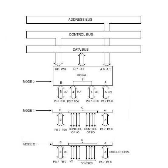
| There are three basic modes of operation that can be selected by the systems software: |
|
Mode O – Basic Input/Output Mode 1 – Strobed Input/Output Mode 2 – Bi-Directional Bus |
|
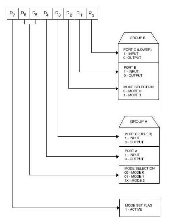
When the reset Input goes “high” all ports will be set to the Input mode (i.e., all 24 lines will be in the high Impedance state). After the reset is removed the 8255A can remain in the input mode with no additional Initialization required. During the execution of the systems program any of the other modes may be selected using a single output Instruction. This allows a single 8255A to service a variety of peripheral devices with a simple software maintenance routine. The modes for Ports A and Port B can be separately defined, while Port C is divided into two portions as required by the Port A and Port B definitions. All of the output registers, including the status flip-flops, will be reset whenever the mode is changed. Modes may be combined so that their functional definition can be “tailored” to almost any I/O stricture. For instance; Group B can be programmed in Mode 0 to monitor simple switch closing or display computational results, Group A could be programmed in Mode 1 to monitor a keyboard or tape reader on an interrupt-driven basis. |
|
|
|
|
|
Figure 6. Mode Definition Format |
| The Mode definitions and possible mode combinations may seem confusing at first but after a cursory review of the complete device operation a simple , logical I/O approach will surface. The design of the 8255A has taken into account things such as efficient PC board layout, control signal definition vs PC layout and complete functional flexibility to support almost any peripheral device with no use of the available pints. |
Single Bit Set/Reset Feature |
| Any of the eight bits of Port C can be Set or Reset using a single OUT put Instruction. This feature reduces software requirements in Control-based applications. |
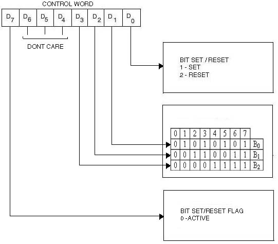 |
| When Port C is being used as status/control for Port A or B these Bits can be set or reset by using the Bit set/reset operation just as if they were data output port. |
Interrupt Control Functions |
| When the 8255A is programmed to operate in mode 1 or mode 2, control signals are provided that can used as interrupt request input to the CPU. The interrupt request signal generated from port C, can be inhibited or enabled by setting or resetting the associated INTE flip-flop, using the bit set/reset function of port C. |
| This function allows the Programmer to disallow or allow a specific I/O device to interrupt the CPU without affecting any other device in the interrupt structure. |
INTE flip-flop definition(BIT-SET) – INTE is SET – Interrupt enable (BIT-RESET) – INTE is RESET – Interrupt disable |
| Note: All Mask flip-flops are automatically reset during mode selection and device reset. |
| Operating Modes |
| Mode 0 (Basic Input/Output).
This functional configuration provides
simple input operations for each of the three ports. No “handshaking”
is required data is simply written to or read from a specified
port. |
| Mode O Basic Functional Definitions: |
|
|
||||||||||||||||||||||||||||||||||||||||||||||||||||||||||||||||||||||||||||||||||||||||||||||||||||||||||||||||||||||||||||||||||||||||||||||||||||||||||||||||||
| MODE
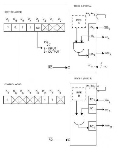
1 (Strobed Input/Output). This functional configuration provides a
means for transferring I/O data to or from a specified port in conjunction
with strobes or “handshaking” signals. In mode 1, port
A and Port B use the lines on port C to generate or accept these “handshaking”
signals. |
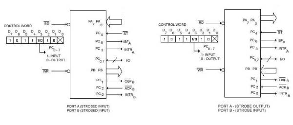
| Mode
1 Basic Functional Definitions: |
|
Input Control Signal Definition
|
| STB (Strobe Input). A “ low “ on the input loads data into the input latch. |
| IBF (Input
Buffer Full F/F) |
|
INTE A Controlled by bit
set/reset of PC4 |
|
INTE B Controlled by set/reset PC2 |
|
|
Output Control
Signal Definition
|
|
OBF (Output Buffer Full F/F). The OBF output will go “low” to indicate that the CPU has written data out to the specified port. The OBF F/F will be set by rising edge of the WR input being low. ACK (Acknowledge Input). A “low” on this input informs the 8255A that the data from port A or port B has been accepted. In essence, a response from the peripheral device indicating that it has received the data output by CPU. INTR (Interrupt Request). A “high” on the output can be used to interrupt the CPU when an output device has accepted data transmitted by the CPU. INTR is set when ACK is a “one”, OBF is a “one”, and INTE is a “one”. It is reset by the falling edge of WR.
|
|
Combination of MODE
1 Port A and B can be Individually defined as Input or output in Mode 1 to support a wide varlety of strobed I/O application. |
|
|
|
Mode 2 (Strobed Bidirectional Bus I/O). This functional configuration provides a means for communicating with a peripheral device or structure on a single 8-bit bus for both transmitting and receiving data (bi-directional bus I/O). “Handshaking” signals are provided to maintain proper bus flow discipline in a similar manner to MODE. 1. Interrupt generation and enable/disable functions are also available. |
|
MODE 2 Basic Functional Definitions: |
|
Bi-directional Bus I/O Control Signal Definition |
| INTR (Interrupt Request). A high on this output can be used to interrupt the CPU for both input or output operations. |
Output OperationsOBF (Output Buffer Full). The OBF output will go “low” to indicate that the CPU has written data out to port A. ACK (Acknowledge). A “low” on this input enables the iri-state output buffer of port A to send out the data. Otherwise, the output buffer will be in the high impedance state. INTE 1 (The INTE Flip-Flop Associated with OBF). Controlled by bit set/reset of PC6 |
Input Operations STB
(Strobe Interrupt) STB (Strobed Input). A “low” on this input loads data into the input latch. IBF (Input
Buffer Full F/F). A “high”
on this output indicates that data has been loaded into the input
latch. INTE 2 (The INTE Flip-Flop Associated with IBF). Controlled by bit set/reset of PC4. |
Pinout
|
Block diagram
8255A BASIC OPERATION
|
A1 |
A0 |
___ RD |
___ WR |
___ CS |
INPUT
OPERATION (READ) |
|
0 |
0 |
0 |
1 |
0 |
PORT
A – DATA BUS |
|
0 |
1 |
0 |
1 |
0 |
PORT
B – DATA BUS |
|
1 |
0 |
0 |
1 |
0 |
PORT
C – DATA BUS |
|
|
|
|
|
|
OUTPUT
OPERATION (WRITE) |
|
0 |
0 |
1 |
0 |
0 |
DATA
BUS – PORT A |
|
0 |
1 |
1 |
0 |
0 |
DATA
BUS -- PORT B |
|
1 |
0 |
1 |
0 |
0 |
DATA
BUS – PORT C |
|
1 |
1 |
1 |
0 |
0 |
DATA
BUS – CONTROL |
|
|
|
|
|
|
DISABLE
FUNCTION |
|
X |
X |
X |
X |
1 |
DATA
BUS – 3 STATE |
|
1 |
1 |
0 |
1 |
0 |
ILLEGAL
CONDITION |
|
X |
X |
1 |
1 |
0 |
DATA
BUS – 3 STATE |
BSR mode
Bit set/reset, applicable to PC only. One bit is S/R at a time. Control word:
| D7 | D6 | D5 | D4 | D3 | D2 | D1 | D0 |
| 0 (0=BSR) | X | X | X | B2 | B1 | B0 | S/R (1=S,0=R) |
Bit select: (Taking Don't care's as 0)
| B2 | B1 | B0 | PC bit | Control word (Set) | Control word (reset) |
| 0 | 0 | 0 | 0 | 0000 0001 = 01h | 0000 0000 = 00h |
| 0 | 0 | 1 | 1 | 0000 0011 = 03h | 0000 0010 = 02h |
| 0 | 1 | 0 | 2 | 0000 0101 = 05h | 0000 0100 = 04h |
| 0 | 1 | 1 | 3 | 0000 0111 = 07h | 0000 0110 = 06h |
| 1 | 0 | 0 | 4 | 0000 1001 = 09h | 0000 1000 = 08h |
| 1 | 0 | 1 | 5 | 0000 1011 = 0Bh | 0000 1010 = 0Ah |
| 1 | 1 | 0 | 6 | 0000 1101 = 0Dh | 0000 1100 = 0Ch |
| 1 | 1 | 1 | 7 | 0000 1111 = 0Fh | 0000 1110 = 0Eh |
![[Pinout 8255]](8255_1_files/pin8255.png)
![[8255 block diagram]](8255_1_files/blk8255.png)