The RISC Concept
1. Introduction
The motivation for the design of RISC processors arose from technological
developments which changed gradually the architectural parameters
traditionally used in the computer industry. Patterson [1985] has already
given a detailed account of the prehistory of RISC.
At the abstract architectural level the general trend until the middle of
the seventies was the design of ever richer instruction sets which could
take some of the burden of interpreting high level computer languages from
the compiler to the hardware. The philosophy of the time was to build
machines which could diminish the semantic gap between high level languages
and the machine language. Many special instructions were included in the
instruction set in order to improve the performance of some operations
and several machine instructions looked almost like their high-level
counterparts. If anything was to be avoided it was, first of all, compiler
complexity.
At the implementation level, microcoding provided a general method of
implementing increasingly complex instruction sets using a fair amount of
hardware. Microcoding also made possible to develop families of compatible
computers which differed only in the underlying technology and performance
level, like in the case of the IBM/360 system.
The metrics used to assess the quality of a design corresponded directly
to these two architectural levels: the first metric was code density,
i.e., the length of compiled programs; the second metric was compiler
complexity. Code density should be maximized, compiler complexity should
be minimized. Not very long ago Wirth [1986] was still analyzing some
microprocessor architectures based exactly on these criteria and denouncing
them for being "halfheartedly high-level language oriented."
There were good reasons for microcoded designs in the past. Memory
was slow and expensive - therefore compact code was required. There
was a need for instructions of high encoded semantic content which
could maintain the processor running at full speed with a minimum of
instruction fetches. Microcode had also an additional advantage: it could
be changed in different models of the same computer family, allowing for
increased parallel execution of individual instructions in the high end
of the family. The transition from the use of core memory (with typical
cycle times 10 times slower than semiconductor memory) to the now used
dynamic and static memory chips eliminated one of the advantages of
microprogramming. Microprograms and real programs could be stored in the
same kind of devices with comparable access times. The introduction of cache
memories in the early seventies altered the equation again in favor of
external programming against microprogramming [Bell 1986].
One of the fundamental elements in the performance equation was still the
instruction set used. IBM, DEC and other companies had installed thousands
of machines by the seventies and compatibility was the really important
issue of every new processor release. The users of IBM products were
locked-in with this company due to their high software investment, but
IBM was also locked-in with their old abstract computer architecture and
instruction set, which still survives today after 26 years of having been
introduced!
It is surprising that the winds of innovation first blew inside IBM. The
project which is now recognized as the first pioneering RISC architecture
was started 1975 at the IBM Research Center in Yorktown Heights, N.Y. A
small computer system, which was intended originally to control a telephone
exchange system, evolved into a minicomputer design which challenged the
traditional computer architecture wisdom [Hopkins 1987]. John Cocke, an IBM
fellow, had noticed that only a small subset of the IBM/360 instruction
set was used most of the time and it was this subset which had the biggest
impact on execution time. Cocke and his colleagues set themselves the goal
of simplifying the instruction set in order to achieve one cycle execution
time as an average. This objective could only be achieved if the instruction
set was pipelined, masking in this way the cycles used for fetching and
decoding of the instructions.
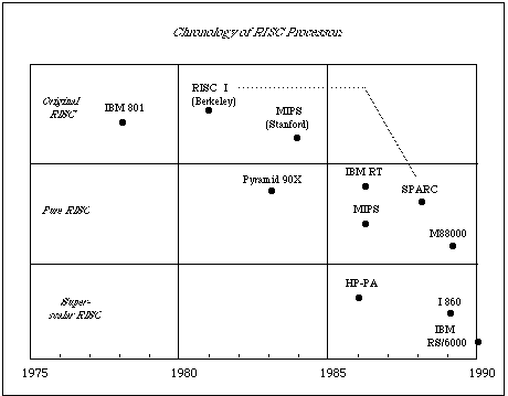
Two projects which started some years later brought RISC concepts finally
into the mainstream of computer architecture. The first one was led by
David Patterson at the University of Berkeley and culminated in the
definition of the RISC-I and RISC-II processors at the beginning of the
eighties. Patterson also coined the RISC acronym. John Hennessy led
simultaneously the MIPS project at Stanford which evolved into a commercial
venture some years later. Figure 1 shows a chronology of the RISC processors
that will be discussed in this survey.
According to Patterson [1985] RISC processors inaugurated a new set of
architectural design principles. Because of this, RISC has been called more
a philosophy than a particular architectural recipe. The relevant points of
this design philosophy mentioned by Patterson are:
- The instruction set must be kept simple
- Instructions must run at the fastest possible rate (without intermediate
interpreting levels like microcode)
- Pipelining is more important than program size
- Compiler technology is a critical ingredient of RISC designs: optimizing
compilers must transport so much complexity from the hardware into the
compiling phase as possible.
(Figure 1)
In this informal account by Patterson there is no clear hierarchy among
these four different objectives. Every one of them seems to be equally
important for a definition of RISC. We will see in the next section, that
assuming a clear hierarchy which puts pipelining at the center of the design
work leads effortlessly to a listing of all relevant RISC traits.
When RISC is understood as just the name of a bundle of architectural
features for processors, the most frequently mentioned are:
- 1) small instruction set
- 2) load/store architecture
- 3) fixed length coding and hardware decoding
- 4) large register set
- 5) delayed branching
- 6) processor throughput of one instruction per cycle in average
The difference between RISC as design philosophy and RISC as a bundle
of features is something which remains obscure in the popular computer
literature. There is no clear view of the interdependence of the diverse
features. Processor throughput, for example, is a dependent variable of
decoding time, but not the other way around. We already mentioned that in
most cases RISC is understood as meaning just a "small" instruction set. In
this spirit some authors have claimed that the first RISC machine was the
PDP-8 with only eight basic instructions, and there is also the talk of an
"ultimate RISC" machine with an instruction set of only one instruction.
There is obviously a widespread misconception of what RISC means and of
the reasons for the greater performance of RISC processors. RISC does not
mean going "back to the future" (as Gordon Bell [1986] once ironically
asked) if that means going back to the old designs. The essence of RISC is
constructing parallel machines with a sequential instruction stream. RISC
designs exploit instruction level parallelism and the distinguishing feature
is an instruction set optimized for a highly regular pipeline flow. This
point has not been perceived clearly outside the computer architecture
community and this survey tries to elucidate this as its first task. When
the essence of RISC has been understood, the absurdity of the claim that
the PDP-8 was the first RISC machine becomes obvious. It is also possible
to evaluate the claims of microprocessor manufacturers who nowadays speak
of their own CISC processors as of camouflaged RISC engines. Although the
essence of RISC is parallelism, RISC surveys have systematically avoided
giving empirical data on the effective level of pipelining achieved with the
old and the new architectures [Gimarc/Milutinovic 1987, Horster et al 1986].
2. The RISC principles
Parallel computers seem to be the promise of the future, yet there are few
who pause to realize that they are the computer systems that we are using
now. The sequential processor belongs to the past of computer technology
and today it is used only in small systems or special controllers. The main
parallelising method used by modern processors is pipelining.
Uniprocessor systems get their instructions from the main memory in a
sequential fashion, but they overlap several phases of the execution path
of the received instructions. The execution path of an instruction is
the sequence of operations which each instruction must go through in the
processor. The phases in the execution path are typically: instruction
fetch, decode, operand fetch, ALU execution, memory access and write back
of the operation results. In some processors the chain of phases in the
execution path can be subdivided still more finely. Others use a coarser
subdivision in only three stages (fetch, decode, execute). The number
of stages in the execution path is an architectural feature which can
be changed according to the intended exploitation of instruction level
parallelism.
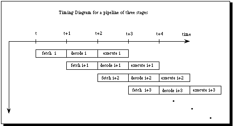
Pipelining is just the overlapped execution of the different phases of the
execution path. Figure 2 shows how a pipeline of depth three is started. It
begins by fetching instruction i in the first cycle. In the second cycle
instruction i is decoded and instruction i+1 is fetched. In the third cycle
instruction i+2 is fetched, instruction i+1 is decoded and instruction i is
executed. The pipeline is then full and if it remains so, turning out one
instruction execution per cycle, the processor works as a parallel processor
capable of speeding up execution by the factor three. We have now in fact a
parallel processor disguised as a sequential one.
In real systems there are many reasons for the regular pipeline flow to be
interrupted systematically. The penalty for these disruptions is paid in the
form of lost or stall pipeline cycles. The effective parallelism exploited
by traditional CISC microprocessors (like the 68030 or Intel 80286) is
rarely larger than the factor 2, and more likely to be near the factor
1.5. This means that old CISC microprocessors offer a very limited form of
instruction level parallelism.
(Figure 2)
The main difference between RISC and CISC, is that the instruction set of
the first kind of processors was explicitly designed to allow the sustained
execution of instructions in one cycle as average. CISC processors (in
mainframes) can also approach this objective, but only at the expense of
much more hardware logic capable of reproducing what RISC processors achieve
through a streamlined design. Some RISC processors, like the SPARC, achieve
a sustained speedup of 2.8 running real applications. This means that the
SPARC is a parallel engine capable of working on about three instructions
simultaneously. Other RISC processors offer similar performance.
The "official" definition of RISC processors should thus be: processors with
an instruction set whose individual instructions can be executed in one
cycle exploiting pipelining. Pipelined supercomputers and large mainframes
have used pipelining intensively for years, but in a radically different way
as RISC processors [Hwang/Briggs 1985]. In IBM mainframes, for example, the
instruction set was given by "tradition" and pipelining was implemented in
spite of an instruction set which was not designed for it. Of course there
are ways to accommodate pipelining, but at a much higher cost. This is the
reason why other pipelined mainframes, like the CDC/6600, are seen as the
precursors of RISC machines rather than the IBM/360 behemoths.
In summary: taking pipelining as the starting point, it is easy to deduct
all other features of RISC processors. The fundamental question is: what is
needed in order to maintain a regular pipeline flow in the processor? The
following RISC features constitute the answer:
a) Regular pipeline phases and deep pipelines
First of all the logical levels of the processing pipeline must be defined
and each one must be balanced against each other [Hennessy/Patterson
1990]. Going through each pipeline stage must take the same time and all the
work done in the execution path should be distributed in the most uniform
way. Each pipeline stage takes a complete clock cycle. Typical processors
use a clock cycle time at least so large as the time it takes to perform
one typical ALU operation. In a processor with 20 MHz clock rate each
cycle lasts 50 nanoseconds. Using standard CMOS technology in the logic
components, this is equivalent to about 10 logic levels (each logic level
has a delay of 5 ns). It is clear that this restriction imposes a heavy
burden on the designer of microprocessors. In each stage of the pipeline a
maximum of 10 logic levels can be traversed. The computer architect must
try to parallelise each one of the phases internally in order to use a
minimum of logic levels. This is easier if the pipeline phases are correctly
balanced and if they are as independent from each other as possible, so as
not to have to handle signals running from one stage to the other. Typical
RISC processors go beyond the classical three level pipeline and use
pipelines with four, five or six levels. A deeper pipeline means more
potential parallelism but also more coordination problems. We return to this
problem later.
b) Fixed instruction length
In CISC processors, like the VAX, instructions are of variable length
and several words have to be fetched until the whole instruction can be
completely decoded. This introduces a variable element in the duration
of the fetch stage which can stall the pipeline if the decoding stage
is waiting for an instruction. Large processors avoid this problem with
a prefetch buffer which can store many instructions of the sequential
stream. CISC microprocessors use also small prefetch buffers or several
words of instruction cache like is the case with the Motorola 68020.
The simplest technique for avoiding a variable fetch time is to encode
each instruction using a fixed one word format. The fetch stage has in
this way a fixed duration and one instruction can be issued each cycle to
the decoding stage under normal pipeline flow (the branching problem is
considered below). The decoding stage does not need to request additional
instruction bytes according to the encoding of the instruction and there
is no need for any additional control lines between the fetch and decode
stages.
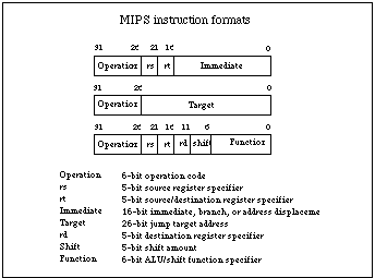
c) Hardwired decoding
A fixed instruction format also makes the decoding of instructions easier. Typical
RISC processors reserve 6 bits out of 32 for the opcode of the instruction (which
makes it possible to encode 64 instructions). The operands and the result are
typically held in registers. Each argument is encoded, using for example 5 bits.
Thirty-two registers can be referenced in this way. Decoding of the opcode and
access to the register operands can be done simultaneously, which is a very important
feature if the operands are to be ready for execution in the next cycle. Figure
3 shows the encoding format of the MIPS processor, a typical RISC engine.

(Figure 3)
Note that in case one of the operands is a constant (that must be stored
or added to in a register) it is encoded using an overlapped format. This
poses no problem for the decoder, because this constant can be decoded
simultaneously with the access to the argument registers. One register too
much will be read, but this intermediate read can be discarded without
losing any cycles. As can be seen, decoding of a fixed instruction format
can be done in parallel in a clock cycle.
d) Register to register operations
The execution phase of an instruction should also take one clock cycle
as a maximum whenever possible. Arithmetical instructions which access
operands in memory do not fulfill this condition because the long latency
of memory accesses keeps the ALU waiting several cycles. Register to
register operations avoid this inconvenience. This kind of instruction
can be executed almost always in one cycle using the 10 levels of logic
available in a pipeline stage of a 20 MHz processor. Instructions like
integer multiply or divide can be directly implemented in the ALU, but they
take several cycles to complete and they inevitably stall the pipeline. Some
RISC processors, like the SPARC, do not directly implement multiply and
divide. The corresponding routines have to be implemented in software. CISC
processors, like the VAX or the 68020 admit registers to memory operations
with a long latency and which introduce large pipeline "bubbles."
e) Load/store architecture
If all operands for arithmetic and logical operations are located in
registers, it is obvious that these registers have to be loaded first
with the necessary data. This is done in RISC processors using a "load"
instruction, which can access bytes, halfwords or complete words. A "store"
instruction transfers the contents of registers to memory.
Without special measures the processor must wait after each load instruction
for the memory to deliver the wished data - the pipeline stalls. RISC
processors avoid this problem using a "delayed" load. The load instruction
is executed in one cycle but the result of the load is made available only
one or more cycles later. This means that the instruction following the
load must avoid using the register being loaded as one of its arguments. In
most cases this condition can be enforced by the compiler, which tries to
reschedule the instructions so that the load does not have to stop the
pipeline. When this rescheduling is not possible, the load stalls the
pipeline for as many cycles as the main memory or cache takes to respond.
f) Delayed branching
The most complex hazard menacing the uninterrupted pipeline flow is
branching. Instructions are fetched sequentially but a taken branch can
alter the sequential flow of instructions. After a taken branch a new
instruction located at the branch target has to be fetched and the pipeline
has to be flushed of now irrelevant instructions. Statistics of real
programs have shown that 15% of all instructions for some processors can
be branches [Hennessy/Patterson 1990]. Around half of the forward going
branches and 90% of the backward going branches are taken. This amounts
to many lost pipeline cycles in typical CISC processors, which flush the
pipeline after each taken branch.
RISC processors use other strategies. First of all, the branching decision
is made very early in the execution path - possibly already in the decode
stage. This can be done only if the branching condition tests are very
simple, like for example a register compare with zero or a condition flag
test. At the end of the decode phase the processor can start fetching
instructions from the new target. But in this decode cycle the next
instruction after the branch has already been fetched. In order to avoid
stall cycles this instruction can be executed. In this case the branch is a
delayed branch. From the programmers point of view the branch is postponed
until after the next instruction is executed. The compiler tries to schedule
a useful instruction in the location after the branch, which is called the
"delay slot." Some RISC processors with very deep pipelines schedule up
to two delay slots [McFarling/Hennessy 1986]. More delay slots make the
scheduling of useful instructions increasingly complicated and in many cases
the compiler ends writing NOPs in them.
It must be said in justice that delayed branching is not strictly a RISC
innovation. This kind of branching was used before in microprograms but
certainly not in macroinstruction sets.
Another technique borrowed from mainframes is the so called "zero cycle"
branching. After each prefetch of a branch special hardware tries to
predict if the branch will be taken or not. The next instruction is then
prefetched from the predicted target address. In this case no delay slots
are needed. If a special branching processor is included (like in the IBM
RS/6000 RISC system) branches can be preprocessed and filtered out so that
the arithmetical processor receives only a sequential instruction stream
[Oehler/Groves 1990]. A good prediction strategy can maintain the pipeline
flowing almost without disruption.
g) Software scheduling and optimizing compilers
The interaction between delayed loads and delayed branching can be very
complex. The whole benefit of a RISC architecture can be reaped only if
the compiler is sophisticated enough to rearrange instructions in the
optimal order. RISC architectures try to maximize the synergy between
hardware and software. Optimizing compilers are thus not an optional
feature of RISC systems but one of their essential components. C compilers
especially, have become sophisticated enough to outperform hand coding in
assembly language. Our own programming experiments using a SPARC workstation
brought a run time improvement of at most 3% with hand corrections to the
assembly code of C programs. This is very different than the situation with
traditional high level compilers for CISC machines, where hand coding can
improve compiled code dramatically. Using the same benchmarks as with the
SPARC workstation, we were able to speed up compiled code in a MicroVax by
almost 100% using hand coding!
h) High Memory Bandwidth
If instructions are to be fetched, decoded and executed in one cycle steps,
a huge memory bandwidth is required. Using a 20 MHz processor and dynamic
RAM chips with 100 ns cycle time some form of intermediate cache is needed,
capable of delivering at least one word per cycle. RISC processors depend on
a complex memory hierarchy in order to work at full speed. In most of them,
separate data and instruction caches try to avoid contention for the system
bus when a fetch is overlapped with a register load or store. For this
reason most RISC processors include memory management components. A RISC
processor without management of a memory hierarchy could hardly outperform a
CISC processor because the latter encode much more semantic information in
each instruction [Flynn et al 1987].
From the above discussion it should be clear that all of the discussed
RISC features are part of a common strategy to guarantee an uninterrupted
pipeline flow, and in this way, a high level of parallel execution of
sequentially coded programs. Fixed word encoding, hardwired decoding,
delayed loads, delayed branches, etc., are just ways to achieve a regular
pipeline flow. Some of these features could disappear in future RISC designs
(for example in processors with zero cycle branching no delayed loads are
necessary) or not be used in others (the floating point units of RISC
processors are sometimes microcoded). The essential point will remain being
the exploitation of instruction level parallelism.
How much instruction level parallelism do typical programs contain? It is
not possible to give a definite answer to this question, because it depends
on the instruction set used. Instruction sets can be designed with the
pipeline flow or with other objectives in mind. Reduced instruction sets
have one clear objective: minimizing pipeline stalls, and for this reason
they can exploit instruction level parallelism more intensively than CISC
processors. There is widespread disagreement in the literature about the
instruction level parallelism available in real programs. Some authors
calculated in the seventies that a maximum speedup by a factor of 2 could
be achieved using this form of parallelism. More recent results suggest
that the available average parallelism could be as large as a factor of 5
[Wall 1991]. Other groups have reported experiments in which the available
parallelism for processors with multiple execution units fluctuated between
2 and 5.8 instructions per cycle [Butler et al 1991]. With an unbounded
machine size it was possible to achieve parallelising rates of 17 to
1165 instructions per cycle! More conservative estimates reckoned that
normal pipelined processors were already using almost all of the available
parallelism [Jouppi/Wall 1989]. Excessive pipelining can also reduce the
overall performance in some cases [Smith/Johnson/Horowitz 1989]. More
research is needed about this important problem before an upper limit for
the available instruction level parallelism can be agreed upon.
3. Taxonomy of RISC processors
A compact but precise discussion of the features of commercial RISC
processors presupposes some kind of classification method. A taxonomy of the
most important aspects of the architecture is needed. In what follows we
develop such a taxonomy considering the most relevant characteristics that
should be taken into account when discussing RISC designs.
The simplest method to achieve this is to use a top-down approach, in which
successive features are examined by focusing the attention in ever finer
subsets of the computer architecture. Following this approach we come to the
architectural characteristics discussed below.
Word width
The first important feature of the processor and memory ensemble is the
word width used by the processor. Most current RISC processors use a 32 bit
internal and external word width. This means that the integer registers,
the address and data paths are restricted to this number of bits. There
are nevertheless a few RISC processors which already use a partial 64 bit
architecture. The Intel 860 processor, for example, has a bus control unit
capable of reading or writing 64 bits simultaneously to memory. The IBM
RS/6000 processor uses thirty-two 64 bit floating point registers. Probably
the first full fledged 64 bit processor will be the MIPS R4000 processor,
which could be announced in 1992.
Split or common cache
RISC processors need a cache between them and main memory. But this cache
can be a common one, in which instructions and data are mixed, or it can be
a split unit, in which two separate caches hold respectively instructions or
data. The efficiency of both caching methods is very similar, but the split
approach is used in many RISC designs.
On-chip or off-chip cache
Some RISC processors use an on-chip cache because it is faster to access,
although it increases the chip complexity and therefore the chip area. Other
processors were designed with an off-chip cache in mind (like the SPARC
chip), in order to simplify the design of the integer unit. CISC processors,
like the Intel 80486, use an on-chip cache in order to cut the performance
advantage of RISC processors.
Harvard or Princeton architecture
In systems with a split cache it is possible to use separate data and
address buses for each cache separately. In this case an instruction fetch
can be handled in parallel with a data access. This is called a Harvard
architecture. A Princeton architecture uses a common bus to access data
and instruction cache. The Motorola 88000 employs a Harvard architecture,
whereas the MIPS R3000 chip uses a Princeton architecture. The MIPS chip
multiplexes the use of the common cache bus between the fetch unit and the
data unit. It should be noticed that a Harvard architecture does not mean
separate buses from the cache to main memory. From the processor to the two
cache units two buses are used, but the cache units share a single bus to
main memory.
Prefetch buffer
The instruction stream to the processor can be handled with an additional
level in the memory hierarchy. Fast prefetch buffers can access the
instruction cache sequentially in advance in order to hold several
instructions ready to be consumed by the processor. This structure is called
a prefetch buffer. Only few RISC processors use prefetch buffers. The IBM
RS/6000 is one of them. It works with a prefetch buffer capable of storing 4
instructions. This kind of buffer is very important for processors which try
to achieve the maximal instruction issue rate.
Write buffer
The equivalent to prefetch buffers on the data stream side are write
buffers. The processor does not have to wait until some data has been
written on the cache. It just gives a write request to the write buffer and
special hardware handles the request autonomously.
Coprocessor or multiple units architecture
This is one of the decisive classification criteria for RISC processors. A
coprocessor architecture means that the instruction stream is analyzed
concurrently by two or more processors (for example an integer processor
and a floating point processor). Each processor takes the instructions that
it can handle, the others interpret it as a NOP. In this way integer and
floating point operations can be executed concurrently in two different
processors. The processors can communicate through memory or through special
control lines.
A multiple unit architecture means that there is a central decoding facility
which starts execution units according to the instruction which has been
decoded. The decoding unit, for example, can start an integer addition
in the integer unit - one cycle later it can start the floating point
multiplication unit, and so on.
The Motorola 88000 and the IBM RS/6000 use a multiple unit architecture,
whereas the SPARC and MIPS chip sets use a coprocessor architecture.
Common register file or private registers
In a coprocessor architecture each processor handles its own registers
and register interchange is managed thorough memory. In a multiple unit
architecture there are two possibilities: a common register file can be
accessed by all execution units or the execution units themselves can
work with private registers. A combination of these two extremes is also
possible. The Motorola 88000 is a processor with a common register file. The
IBM RS/6000 uses private registers in its execution units.
Width and number of internal data paths
The performance of execution units can be enhanced by using more and
wider datapaths in the internal architecture of a processor. It makes a
performance difference if 64 bits have to be transferred from the registers
in one or two 32 bit steps. Two write-back paths to the register file are
better than one mainly in processors with multiple units.
Condition codes
Control of execution flow has been achieved traditionally through the use
of condition bits which are set as a side effect of some arithmetical or
logical operations. Several RISC processors set condition bits explicitly
in one of the general purpose registers. This register can then be tested
by the branching instruction. This strategy avoids the problems associated
with a long pipeline in which it is not completely clear which instruction
changed the condition codes the last time. IBM solved this problem by
multiplying the number of condition bits: up to ten sets of condition codes
are available in the IBM RS/6000.
Register renaming and scoreboarding
In RISC processors the management of the register file is an essential
feature. There are three different ways to solve the scheduling problem
for the usage of registers: the first solution is to schedule registers
in software and to avoid collisions through a sophisticated compile time
analysis. The second solution relies on the help of a special hardware
"scoreboard" that tracks the usage and availability of registers. Whenever
a register which is not yet free is requested, the scoreboard locks the
request until the register is available. The third solution comes from
the mainframe world and was implemented by IBM in the RS/6000 processor:
registers are dynamically renamed by the hardware. If two instructions need
register R2 to generate a temporary result, one of the two gets access to
this register and the other to a "copy" of R2. The results are calculated
and the real R2 is updated according to the sequential order of the calling
instructions. A full explanation of this technique can be found in the book
of Hennessy and Patterson [1990].
Pipelining depth of multiple units
In chips with multiple units an important parameter is the pipeline depth
of each unit. Floating point units are implemented with a deeper pipeline,
taking into account the longer latency of floating point operations. An
important question is how the pipelines of different depth are coordinated
so as to avoid collisions at the exit of the pipelines, when more than one
unit could try to access the register file.
Chaining
Another important question is if the output of execution units is to be
directly connected to the input of other execution units. If this is the
case something similar to the so called "chaining" of vector processors is
available. The multiplier, for example, can be directly connected to an
adder and in this way the inner product of two vectors can be calculated
extremely fast.
Multiple purpose architecture
The last architectural feature of interest is if the processor being
considered exhibits a general purpose architecture or not. A general purpose
chip needs to implement interrupts, protection levels and uses a memory
management unit. Almost all RISC processors provide these features. The ones
that do not provide them have been designed for embedded applications or for
simple multiprocessing nodes (like the Transputer).
After this summary of architectural features the structure of real computers
can be discussed.
4. Survey of features of commercial RISC processors
In this section we review some of the most important and popular RISC
processors. We limit ourselves to summarizing the relevant features of
each design. We have also drawn for each processor the corresponding
Kiviat graph. This type of graphical representation has been used in other
architectural studies [Siewiorek/Bell/Newell 1985] and in many fields in
which the representation of several dimensions of data must be handled in
just two dimensions. In doing this we tried to make the design of the Kiviat
graph as expressive as possible in order to facilitate the comparison of
different kinds of processors. It is well known that a graphical approach
can be superior to complicated tables when several data dimensions are
involved [Tufte 1990].
The variables considered in the comparison of processors are the
following: number of pipeline stages, number of addressing modes, number
of instructions, method of branch handling, average CPI according to some
authors, number of registers, instruction length (fixed or variable) and
levels of decoding (one level for hardware decoding, two for microcode,
and three for micro plus nanocode). The circle meets the points in the
different data axis that could be considered as "typical" RISC values. A
pipelining depth of four stages, for example, could be considered as a
normal feature of RISC technology. More pipelining makes the processor
potentially faster if the other associated features have the adequate
values. One single addressing mode is normally associated with a load/store
architecture. Several RISC processors use just 6 bits for the encoding of
instructions: this means that only 64 instructions can be encoded. One
delayed branch slot could be considered normal in most RISC designs, but
there are other alternatives. The IBM RS/6000 for example uses a powerful
branch handling method superior in average to delayed branching, but which
is also more hardware intensive. Thirty-two registers are typical for most
RISC designs.
With this information in mind we can look now at several commercial RISC
processors.
4.1 The MIPS series
The commercial MIPS processor (R2000 or R3000 which differ in the clock rate
and implementation but not in the main architectural features) is a spin-off
from the experimental designs made at Stanford University in the early
eighties. The acronym "MIPS" reveals clearly the design philosophy which
was applied: MIPS stands for Microprocessor without Interlocking Pipeline
Stages. The objective of the MIPS designers was to produce a RISC processor
with deep pipelining and pipeline interlocking controlled by software. If
one instruction requires two cycles to complete, it is the duty of the
compiler to schedule one NOP instruction following it. In this way the only
pipeline bubbles which arise during execution are the NOPs scheduled by the
software, and the hardware does not have to stop the pipeline every now and
then. This reduces the amount of hardware needed in the processor [Thurner
1990].
Some other interesting concepts were explored at Stanford with MIPS-X, a
derivative of the MIPS architecture with additional features [Chow/Horowitz
1987]. Many of them were later adopted in the commercial MIPS processor.
The MIPS R2000 is a 32 bit processor with an off-chip split cache
for instructions and data. A write buffer handles all data writes to
memory. The R2000 uses a common bus to the external caches - it is a non
Harvard architecture. The MIPS chip set follows a radical coprocessor
architecture. The integer CPU is separated from the so called System Control
Coprocessor, which is an on-chip cache control. The CPU and floating point
unit communicate through memory. There are 32 general purpose integer
registers and 16 separate 64 bit floating point registers. The floating
point coprocessor contains an add, a divide, and a multiply unit. There are
no condition code bits and no scoreboard. Register scheduling is managed by
the software [Kane 1987].
Figure 4 shows that the MIPS series approaches the typical RISC circle very
closely. The integer pipeline has a depth of five stages and the floating
point pipeline a maximal depth of six stages. The Cycles per Instruction
(CPI) reported by some studies is 1.7 [Bhandarkar/Clark 1991]. For the ECL
version, the R6000, the reported CPI is 1.2 [Haas 1990].
The MIPS processors have only one addressing mode. The compiler optimizes
the allocation of registers in order to fully exploit the register
file. This is not so efficient as register windows, but the MIPS compiler
does a good job at eliminating unnecessary register loads and stores
[Cmelik/Kong/Ditzel/Kelly 1991].
The total number of instructions is bounded by the six bits available for
the opcode (64 instructions). The processor uses delayed branch with one
delay slot.
The processor is fully hardwired, including the floating point unit. The
low gate count of the MIPS design made it also a good target for faster
chip technology and one ECL processor is already being offered. It was also
targeted for a GaAs implementation.
From the data shown it follows that the MIPS series is one of the cleanest
RISC designs being offered at the time of this writing [Gross et al 1988].
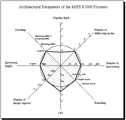
(Figure 4)
4.2 The SPARC family
The SPARC (Scalable Processor Architecture) can claim to descend
from an illustrious lineage. SPARC was derived from the RISC-I and
RISC-II processors developed at the University of Berkeley in the early
eighties. The architecture was defined by Sun Microsystems but it is not a
proprietary design. Any interested semiconductor company can get a license
to build a SPARC processor in any desired technology. In what follows the
design parameters of the Cypress SPARC chips are discussed [Cypress 1990].
The SPARC is a 32 bit processor with an off-chip common cache. Three chips
provide the functionality needed: one for the integer unit, one for the
floating point unit, and another works as a cache controller and memory
management unit. The SPARC design follows the coprocessor architectural
paradigm. Floating point unit and integer unit exchange information through
memory and through some control lines. There is no prefetch buffer. A common
integer register file with two read and one write port is used. The floating
point unit provides 32 registers 32 bits wide. Instructions are decoded in
parallel by the integer and floating point unit. Floating point instructions
are then started when the integer unit sets a control line. Condition
codes are used and no scoreboard is available to control the scheduling of
registers.
Figure 5 shows that SPARC is also a typical RISC oriented design. There are
just two peculiarities that set it apart from other RISC processors. First
of all: the SPARC uses the concept of "register windows" in order to
eliminate the load and stores to a stack associated with procedure
calls. Instead of pushing arguments in a stack in memory, the calling
procedure copies registers from one register window to the next. Register
windows are a hardware oriented method to optimize register allocation. Some
critics of register windows point out that the same benefits can be obtained
by scheduling registers at compile time. The Berkeley team used register
windows because they lacked the compiler expertise needed to implement
interprocedural register allocation, as they later pointed out themselves.
Another peculiarity of the SPARC are its "tagged" instructions. Declarative
languages like Lisp or Prolog make extensive use of tagged data types. The
SPARC provides instructions which make easier to handle a two bit tag in
each word of memory [Cypress 1990]. This feature can speed up Lisp by some
percentage points.
The CPI of the SPARC is 1.6, as confirmed by our own measurements. This is
not significantly different from the CPI of the MIPS series. In all other
architectural respects, the SPARC is very similar to the MIPS machine. Just
the number of addressing modes is higher: two in the SPARC for just one in
the MIPS processor.
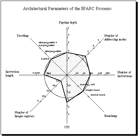
(Figure 5)
4.3 The IBM RS/6000
The IBM RS/6000 or POWER architecture (Performance Optimization with Enhanced
RISC) contains so many innovations compared to the MIPS and SPARC designs, that
it is difficult to say that it is still just another RISC processor. The IBM
RS/6000 shares with older RISC designs the streamlined approach to pipelined
execution. But the instruction set of the IBM processor is large and many special
instructions have been provided in order to speed up execution. The POWER chip
set is indeed an impressive computing engine.
The RS/6000 is a 32 bit processor. Split external caches are used. The processor
follows a Harvard architecture with separate buses for instructions and data.
The first surprise is the width of the instruction buffer: 128 bits are read
in parallel and stored in a 4 word prefetch buffer. The data bus is 64 bits
wide in order to read and store 64 bit floating point data in a single cycle.
The RS/6000 architecture is one of multiple units and consists of three main
blocks: one for control and branching, one for integer operations and another
for floating point. The branching unit tries to detect branches very early by
parsing the prefetch buffer and trying to determine if the branch will be taken
or not. The branching unit runs ahead of the other processing units and in many
cases it can "absorb" the branch instruction, saving one pipeline slot. Because
of this feature IBM names this technique "zero cycle branching" [Oehler/Groves1990].
The floating point unit provides 32 registers 64 bits wide. The registers can
be locked in order to control its utilization by concurrent floating point operations.
One addition and one multiplication can be started concurrently. The processor
is also capable of performing one multiply-and-add operation in four cycles.
This capability is important for the calculation of the scalar product of vectors
and other common mathematical functions. All floating point operations comply
with the IEEE standard.
The Kiviat graph should be explained more carefully. There are in the IBM RS/6000
two different pipelines: one for the integer (called fixed point) and one for
the floating point unit. The first two pipeline stages occur in the branching
unit. The fixed point unit works with four additional stages and the floating
point unit with six [Grohoski 1990]. Integer operations then go through six
pipeline stages and floating point operations through eight. This is a level
of pipelining uncommon in workstations. Other RISC processors do not employ
so deeply pipelined floating point units.
The RS/6000 has one addressing mode and an additional autoincrement mode. The
autoincrement mode is more typical of CISC processors, but it was included in
the RS/6000 to gain some speed trying to avoid compromising the pipeline flow
[Hall/O'Brien 1991]. The additional addressing mode makes the hardware more
complex.
The IBM RS/6000 has no delayed slots because it does not need them. Its branching
lookahead technique makes them irrelevant. The branching unit also owns special
registers and one for iteration counting. With the help of this register the
execution unit does not have to count the number of iterations in a FOR loop,
and only serial code is passed over from the branching to the execution units.
The instruction length of the RS/6000 is fixed but some operations are handled
in microcode (specially FP operations). There are ten sets of condition codes.
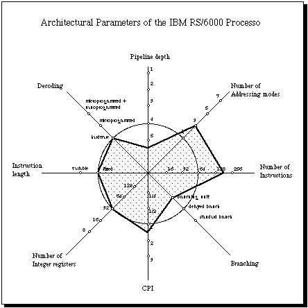
(Figure 6)
One important feature of the RS/6000 is the use of register renaming in the
floating point unit. Through it the processor is able to do loop unrolling
on the fly and achieves execution rates similar to the ones of vector
processors.
The IBM RS/6000 is a superscalar machine because the execution of floating
point and integer operations can be highly overlapped. In some benchmarks
the IBM RS/6000 approaches a CPI of almost 1.1 and the geometric average of
the CPI measured in 9 of the SPEC benchmarks is 1.6 [Stephens et al 1991].
The complexity of the IBM RS/6000 shows itself in the large number of
transistors needed to implement the architecture: more than 2 million just
for the logic! The extra memory required in the different units contributes
other 4.8 million transistors, but most of them are the ones needed in the
caches. This complexity makes it questionable if the architecture can be
scaled up to other technologies (like ECL) which dissipate more energy per
gate.
4.4 The Motorola 88000 family
The 88100 processor, the first in the 88000 family, was launched in 1988 as
the answer of Motorola to the burgeoning RISC designs [Hennessy/Patterson
1990]. The 88000 family sacrificed compatibility with the older 68000 family
for performance. The Kiviat graph below shows the main features of the
M88100.
The 88100 is a RISC processor with a 32 bit external and internal
architecture. Split caches are handled off-chip by two separate 88200 cache
management units. There are separate buses for instruction and data, i.e.,
the processor follows a Harvard architectural model. There is no prefetch
buffer and the processor follows the multiple units approach. There is
one integer unit and two floating point units (adder and multiplier). The
register file is common to all units and contains 32 registers of 32
bits. Register 0 is hardwired to 0. Registers can contain integer or
floating point data. Special function units could be implemented in later
incarnations of the architecture. There are no condition codes: status
information is handled in registers [Alsup 1990].
The M88100 uses three different addressing modes: register plus offset,
register plus register, and register plus scaled register. The last two
addressing modes provide easy access to arrays in memory.
The number of instructions is 51 and 12 of them are floating point
instructions [Hamacher/Vranesic/Zaky 1990].
The processor uses delayed branches with one branch slot. Normal branches
can be used also. Delayed load is also used: the instruction following a
load to a register must wait one cycle to use this register. Two general
purpose registers are concatenated when 64 bits floating point data is
needed.
The 88100 does not dispose of a full fledged scoreboard to control the usage
of registers. Each register has instead an "in use" bit, which is set every
time the register is waiting to be updated by an instruction which has been
started. The processor checks this bit before starting other instructions
which update the same register.
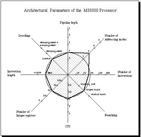
(Figure 7)
The processor works with fixed length instructions and hardware
decoding. There are only four instruction formats, very similar to the
formats of the MIPS R3000 processor. The number of pipeline stages is 4
for integer operations, a more or less typical value for RISC designs. The
pipeline depth of the floating point adder is 4, which together with
instruction fetch and decode give a total pipeline depth of 6.
The Motorola architecture does not offer any other surprises: there are no
register windows nor deviations from a pure RISC approach. The designers
defined a linking convention which allows subroutines to pass parameters
through registers, but this is not equivalent to register windows.
The next member of the family, the M88110, will adopt what Motorola calls a
symmetric superscalar design and will handle branches with a special unit.
4.5 Intel 860
Intel developed the 80860 processor with embedded applications in mind. It
was the first RISC chip of the semiconductor manufacturer and silicon area
was not spared - more than one million transistors were used in the final
design. The chip has not been a great market success.
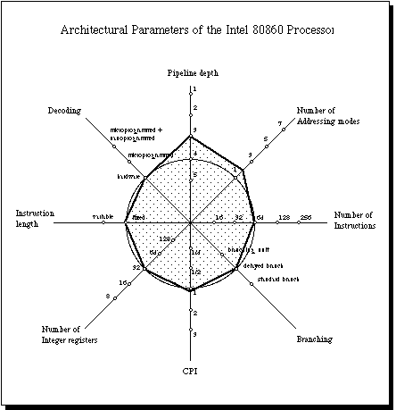
(Figure 8)
The I860 is a 32 bit processor built with a Harvard architecture. The bus to
the instruction cache is 32 bits wide, and the bus to the data cache is 128
bits wide, making possible to access four words in parallel. The caches are
located on-chip [Bodenkamp 1990].
The chip follows the multiple units paradigm and provides one floating point
adder, one floating point multiplier and one special graphics unit. The
"RISC core" contains thirty-two 32 bit registers and one ALU. A scoreboard
controls the allocation of general purpose registers.
The floating point register file contains 30 registers 32 bits wide, which
can be used as 15 64 bit registers. The adding and multiplying units can
be chained to speed-up the multiply and add combination needed in linear
algebra and graphics.
The processor uses a fixed instruction format very similar to the
MIPS format, decoding is hardwired, and only two addressing modes are
provided. The number of instructions is bounded by the six bits provided
for the operation code. Intel reports a CPI of 1.1, but it is more probable
that the CPI lies around 1.6 the "typical" RISC CPI. The pipelines are not
very deep: floating point and integer pipelines have at most three stages,
depending on the unit.
The graphics unit provides some common operations needed to handle single
pixels in computer graphics.
4.6 Hewlett Packard's Precision Architecture
When Hewlett-Packard charged their computer architects with designing a
new processor architecture for the nineties, the goal was set to provide a
single type of machine for commercial and scientific applications across a
large performance range. The new architecture unified the different product
lines of HP and was much more powerful than the older machines.
The Precision Architecture (PA) is a RISC design, which nevertheless
exhibits many characteristics only normally found in larger systems. In this
respect the PA is similar to the Power Architecture of IBM.
The Kiviat graph for the PA systems shows its more relevant features. The PA
is a load/store architecture with fixed instruction length [Lee 1989]. The
number of different instructions formats is larger than in other RISC
machines: twelve different combinations of opcode and register or constant
fields are possible in a single word (the SPARC and MIPS processors use only
four different combinations).
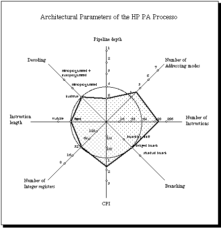
(Figure 9)
The number of different addressing modes is basically two with two
additional modes supporting post- and premodification of an index
register. This gives a total of four different addressing modes.
The number of different addressing modes is basically two with two
additional modes supporting post- and premodification of an index
register. This gives a total of four different addressing modes.
The opcode of the PA consists of six bits. This reduces the number of
possible instructions to less than 64 (although several instructions are
offered in several variants using special bits in the instruction format).
Delayed branches with one slot are used in the PA. The delay slot
instruction can be cancelled according to the result of the branch decision.
The number of general purpose registers in the PA is 32. Thirty-two
additional special purpose registers are also used to manage interrupts,
protection levels, etc.
Some of the above data show that the PA is not a typical RISC design. The
most atypical feature, however, is the low level of pipelining of the
first processors offered. Just three pipeline stages are used [Lee 1989],
although newer designs can employ a deeper pipeline. The pipeline implements
interlocks in hardware. The optimal pipeline flow requires software
scheduling.
The PA achieves a low CPI through simultaneous execution of scalar and
floating point operations. The number of floating point units can vary
from one PA machine to another. The PA tries to achieve a low CPI using
superscalar techniques.
HP's Precision Architecture employs much more hardware than pure RISC
designs trying to achieve a low CPI. The PA philosophy is nearer to the
philosophy of the IBM RS/6000 than to the pure RISC concepts.
Literature:
- [1] Mitch Alsup, "Motorola's 88000 Family Architecture", IEEE Micro,
February 1990, pp. 48-66.
- [2] H.B. Bakoglu, G.F. Grohoski, R.K. Montoye, "The IBM RISC
System/6000 processor: hardware overview", IBM Journal of Research and
Development, Vol. 34, No. 1, January 1990, pp. 12-22.
- [3] Gordon Bell, "RISC: Back to the Future?", Datamation, Vol. 32,
No. 11, June 1 1986, pp. 96-108.
- [4] Dileep Bhandarkar and Douglas W. Clark, "Performance from
Architecture: Comparing RISC and CISC with Similar Hardware Organisation",
Proceedings of the Fourth International Conference on Architectural Support
for Programming Languages and Operating Systems, Santa Clara, California,
April 8-11, 1991, pp. 310-319.
- [5] J. Bodenkamp, "I860 Mikroprocessor", in Arndt Bode (ed),
RISC-Architekturen, Reihe Informatik, Band 60, Wissenschaftsverlag,
Mannheim, 1990, pp. 431-447.
- [6] Emil W. Brown, "Implementing Sparc in ECL", IEEE Micro, February
1990, pp. 10-21.
- [7] Michael Butler, Tse-Yu Yeh, Yale Patt, Mitch Alsup, Hunter Scales,
Michael Shebanow, "Single Instruction Stream Parallelism is Greater than
Two", Proceedings of the 18th Annual International Symposium on Computer
Architecture, ACM, New York, 1991, pp. 276-286.
- [8] Paul Chow and Mark Horowitz, "Architectural Tradeoffs in the Design
of MIPS-X", Proceedings of the 14th Annual International Symposium on
Computer Architecture, Pittsburgh, Pennsylvania, 1987, pp. 300-308.
- [9] Robert F. Cmelik, Shing I. Kong, David R. Ditzel and Edmund
J. Kelly, "An Analysis of SPARC and MIPS Instruction Set Utilization on the
SPEC Benchmarks", Proceedings of the Fourth International Conference on
Architectural Support for Programming Languages and Operating Systems, Santa
Clara, California, April 8-11, 1991, pp. 290-302.
- [10] John H. Crawford, "The i486 CPU: Executing Instructions in One
Clock Cycle", IEEE Micro, February 1990, pp. 27-36.
- [11] Cypress Semiconductor, SPARC RISC User's Guide, February 1990.
- [12] Robin W. Edenfield et al, "The 68040 Processor: Part 1, Design and
Implementation", IEEE Micro, February 1990, pp. 66-78.
- [13] Joel S. Emer, Douglas W. Clark, "A Characterization of Processor
Performance in the VAX-11/780", Proceedings of the 11th Annual International
Symposium on Computer Architecture, Ann Arbor, Michigan, 1984, pp. 301-309.
- [14] Domenico Ferrari, Giuseppe Serazzi and Alessandro Zeigner,
Measurement and Tuning of Computer Systems, Prentice Hall, London, 1983.
- [15] Michael J. Flynn, Chad L. Mitchell and Johannes M. Mulder, "And
Now a Case for More Complex Instruction Sets", Computer, September 1987,
pp. 71-83.
- [16] Charles E. Gimarc and Veljko M. Milutinovic, "A Survey of RISC
Processors and Computers of the Mid-1980s", Computer, September 1987,
pp. 59-69.
- [17] G.F. Grohoski, "Machine organisation of the IBM RISC System/6000
processor", IBM Journal of Research and Development, Vol. 34, No. 1, January
1990, pp. 37-58.
- [18] Thomas R. Gross, John L. Hennessy, Steven A. Przybylski and
Christopher Rowen, "Measurement and Evaluation of the MIPS Architecture and
Processor", ACM Transactions on Computer Systems, Vol. 6, No. 3, August
1988, pp. 229-257.
- [19] Hass, W., "MIPS RISC-Architektur in ECL-Technik", in Arndt Bode
(ed), RISC-Architekturen, Wissenschaftsverlag, Mannheim, 1990.
- [20] Brian Hall, Kevin O'Brien, "Performance Characteristics of
Architectural Features of the IBM RISC System/6000", Proceedings of the
Fourth International Conference on Architectural Support for Programming
Languages and Operating Systems, Santa Clara, California, April 8-11,
1991, pp. 303-309.
- [21] Carl Hamacher, Zvonko Vranesic, Safwat Zaky, Computer
Organisation, McGraw-Hill, New York, 1990.
- [22] John L. Hennessy, David A. Patterson, Computer Architecture A
Quantitative Approach, Morgan Kaufmann Publishers, San Mateo, 1990.
- [23] John L. Hennessy, "What will the single architecture of tomorrow
look like?", Electronic World News, November 5, 1990, pp. c4-c5.65
- [24] M.E. Hopkins, "A Perspective on the 801/Reduced Instruction Set
Computer", IBM Systems Journal, Vol. 26, No. 1, 1987, pp. 107-121.
- [25] Patrick Horster, Dietrich Manstetten and Heidrun Pelzer, Das
RISC-Konzept, Bericht 118, Rheinisch-WestfŠlische Technische Hochschule
AAchen, Juni 1986, 94 p.
- [26] Kai Hwang and Faye A. Briggs, Computer Architecture and Parallel
Processing, McGraw Hill, New York, 1985.
- [27] Norman P. Jouppi, David W. Wall, "Available Instruction-Level
Parallelism for Superscalar and Superpipelined Machines", Proceedings of
the Third International Conference on Architectural Support for Programming
Languages and Operating Systems, Boston, Mass, 1989, pp. 272-282.
- [28] Gerry Kane, MIPS R2000 RISC Architecture, Prentice Hall, Englewood
Cliffs, 1987.
- [29] Ruby B. Lee, "Precision Architecture", Computer, Vol. 22, No. 1,
January 1989, pp. 78-91.
- [30] Scott McFarling and John Hennessy, "Reducing the Cost of
Branches", Proceedings of the 13th Annual International Symposium on
Computer Architecture, Tokyo, Japan, 1986, pp. 396-403.
- [31] Jeff Moad, "Gambling on RISC", Computer, Vol. 32, No. 11, June 1
1986, pp. 86-92.
- [32] Motorola, MC68020 32-Bit Microprocessor User's Manual,
Prentice-Hall, London, 1984.
- [33] R.R. Oehler and R.D. Groves, "IBM RISC System/6000 processor
architecture", IBM Journal of Research and Development, Vol. 34, No. 1,
January 1990, pp. 23-36.
- [34] David Patterson, "Reduced Instruction Set Computers",
Communications of the ACM, Vol. 28, No.1, January 1985, pp. 9-21.
- [35] Omri Serlin, "MIPS, Drystones and Other Tales", in William
Stallings (ed), Reduced Instruction Set Computers, IEEE Computer Society
Press, Washington 1990, pp. 282-296.
- [36] Daniel P. Siewiorek, Gordon Bell and Allen Newell, Computer
Structures: Principles and Examples, McGraw-Hill, Auckland, 1985.
- [37] Michael D. Smith, Mike Johnson and Mark A. Horowitz, "Limits
on Multiple Instruction Issue", Proceedings of the Third International
Conference on Architectural Support for Programming Languages and Operating
Systems, Boston, Mass, 1989, pp. 290-302.
- [38] Chriss Stephens, Bryce Cogswell, John Heinlein, Gregory Palmer,
John P. Shen, "Instruction Level Profiling and Evaluation of the IBM
RS/6000", Proceedings of the 18th Annual International Symposium on Computer
Architecture, ACM, New York, 1991, pp. 180-189.
- [39] E. Thurner, "Die MIPS Prozessor Familie", in Arndt Bode (ed),
RISC-Architekturen, Reihe Informatik, Band 60, Wissenschaftsverlag,
Mannheim, 1990, pp. 379-401.
- [40] Edward R. Tufte, The Visual Display of Quantitative Information,
Graphics Press, Cheshire, 1990.
- [41] David M. Wall, "Limits of Instruction-Level Parallelism",
Proceedings of the Fourth International Conference on Architectural Support
for Programming Languages and Operating Systems, Santa Clara, California,
April 8-11, 1991, pp. 176-189.
- [42] Niklaus Wirth, "Microprocessor Architectures: A Comparison Based on
Code Generation by Compiler", Communications of the ACM, Vol. 29, No. 10,
1986, pp. 978-990.